- 您现在的位置:买卖IC网 > Sheet目录2001 > ISL26134AVZ (Intersil)IC ADC 24BIT SRL 80SPS 28TSSOP
ISL26132, ISL26134
13
FN6954.1
September 9, 2011
Filtering PGA Output Noise
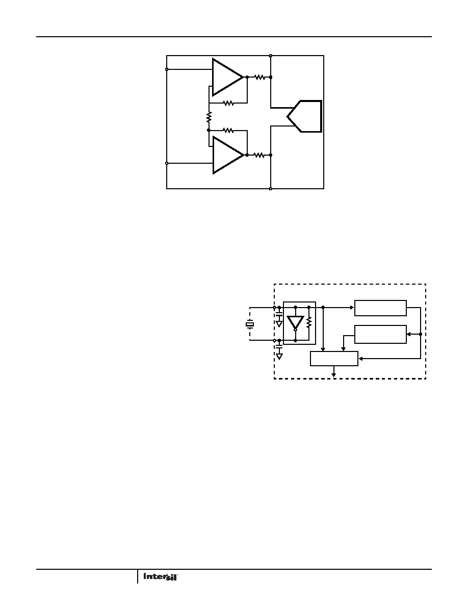
The programmable gain amplifier, as shown in Figure 24,
includes a passive RC filter on its output. The resistors are
located inside the chip on the outputs of the differential amplifier
stages. The capacitor (nominally a 100nF C0G ceramic or a PPS
film (Polyphenylene sulfide)) for the filter is connected to the two
CAP pins of the chip. The outputs of the differential amplifier
stages of the PGA are filtered before their signals are presented
to the delta-sigma modulator. This filter reduces the amount of
noise by limiting the signal bandwidth and filters the chopping
artifacts of the chopped PGA stage.
Voltage Reference Inputs (VREF+, VREF-)
The voltage reference for the ADC is derived from the difference
in the voltages presented to the VREF+ and VREF- pins;
VREF = (VREF+ - VREF-). The ADCs are specified with a voltage
reference value of 5V, but a voltage reference as low as 1.5V can
be used. For proper operation, the voltage on the VREF+ pin
should not be greater than AVDD + 0.1V and the voltage on the
VREF- pin should not be more negative than AGND - 0.1V.
Clock Sources
The ISL26132, ISL26134 can operate from an internal oscillator,
an external clock source, or from a crystal connected between
the XTALIN/CLOCK and XTALOUT pins. See the block diagram of
the clock system in Figure 25. When the ADC is powered up, the
CLOCK DETECT block determines if an external clock source is
present. If a clock greater than 300kHz is present on the
XTALIN/CLOCK pin, the circuitry will disable the internal oscillator
on the chip and use the external clock as the clock to drive the
chip circuitry. If the ADC is to be operated from the internal
oscillator, the XTALIN/CLOCK pin should be grounded.
If the ADC is to be operated from a crystal, it should be located
close to the package pins of the ADC. Note that external loading
capacitors for the crystal are not required as there are loading
capacitors built into the silicon, although the capacitor values are
optimized for operation with a 4.9152MHz crystal.
The XTALOUT pin is not intended to drive external circuits.
Digital Filter Characteristics
The digital filter inside the ADC is a fourth-order Siinc filter.
it is operated from a 4.9152MHz crystal. The internal oscillator is
factory trimmed so the frequency response for the filter will be
much the same when using the internal oscillator. The figures
illustrate that when the converter is operated at 10Sps the digital
filter provides excellent rejection of 50Hz and 60Hz line
interference.
FIGURE 24. SIMPLIFIED PROGRAMMABLE GAIN AMPLIFIER BLOCK DIAGRAM
+
-
A1
-
+
A2
AINx-
AINx+
ADC
RINT
R1
RF1
RF2
CAP
FIGURE 25. CLOCK BLOCK DIAGRAM
XTALIN/
CRYSTAL
OSCILLATOR
XTALOUT
TO ADC
INTERNAL
OSCILLATOR
CLOCK DETECT
MUX
EN
CLOCK
发布紧急采购,3分钟左右您将得到回复。
相关PDF资料
ISL26319FVZ-T7A
IC ADC 12BIT SRL/SPI 16TSSOP
ISL26329FVZ
IC ADC 12BIT SPI/SRL 16-TSSOP
ISL2671286IBZ
IC ADC 12BIT SPI/SRL 20K 8SOIC
ISL26712IRTZ
IC ADC 12BIT SAR 1MSPS 8-TDFN
ISL267450AIUZ
IC INTERFACE
ISL267817IUZ
IC INTERFACE
ISL32272EIVZ-T
IC TX RS422 QUAD 16TSSOP
ISL32273EIVZ
IC RCVR RS485/422 QD ESD 16TSSOP
相关代理商/技术参数
ISL26134AVZ-T
功能描述:模数转换器 - ADC ISL26134AVZ LW-NOISE 24-BIT TI-COMP D/S RoHS:否 制造商:Texas Instruments 通道数量:2 结构:Sigma-Delta 转换速率:125 SPs to 8 KSPs 分辨率:24 bit 输入类型:Differential 信噪比:107 dB 接口类型:SPI 工作电源电压:1.7 V to 3.6 V, 2.7 V to 5.25 V 最大工作温度:+ 85 C 安装风格:SMD/SMT 封装 / 箱体:VQFN-32
ISL26134AVZ-T7A
功能描述:模数转换器 - ADC ISL26134AVZ LW-NOISE 24BIT DELTASIGMA ADC RoHS:否 制造商:Texas Instruments 通道数量:2 结构:Sigma-Delta 转换速率:125 SPs to 8 KSPs 分辨率:24 bit 输入类型:Differential 信噪比:107 dB 接口类型:SPI 工作电源电压:1.7 V to 3.6 V, 2.7 V to 5.25 V 最大工作温度:+ 85 C 安装风格:SMD/SMT 封装 / 箱体:VQFN-32
ISL26310
制造商:INTERSIL 制造商全称:Intersil Corporation 功能描述:12-bit, 125kSPS Low-power ADCs with Single-ended and Differential Inputs and Multiple Input Channels
ISL26310FBZ
功能描述:IC ADC 12BIT SPI/SRL 125K 8SOIC RoHS:是 类别:集成电路 (IC) >> 数据采集 - 模数转换器 系列:- 产品培训模块:Lead (SnPb) Finish for COTS
Obsolescence Mitigation Program 标准包装:250 系列:- 位数:12 采样率(每秒):1.8M 数据接口:并联 转换器数目:1 功率耗散(最大):1.82W 电压电源:模拟和数字 工作温度:-40°C ~ 85°C 安装类型:表面贴装 封装/外壳:48-LQFP 供应商设备封装:48-LQFP(7x7) 包装:管件 输入数目和类型:2 个单端,单极
ISL26310FBZ-T
功能描述:IC ADC 12BIT SPI/SRL 125K 8SOIC RoHS:是 类别:集成电路 (IC) >> 数据采集 - 模数转换器 系列:- 产品培训模块:Lead (SnPb) Finish for COTS
Obsolescence Mitigation Program 标准包装:250 系列:- 位数:12 采样率(每秒):1.8M 数据接口:并联 转换器数目:1 功率耗散(最大):1.82W 电压电源:模拟和数字 工作温度:-40°C ~ 85°C 安装类型:表面贴装 封装/外壳:48-LQFP 供应商设备封装:48-LQFP(7x7) 包装:管件 输入数目和类型:2 个单端,单极
ISL26310FBZ-T7A
功能描述:IC ADC 12BIT SPI/SRL 125K 8SOIC RoHS:是 类别:集成电路 (IC) >> 数据采集 - 模数转换器 系列:- 产品培训模块:Lead (SnPb) Finish for COTS
Obsolescence Mitigation Program 标准包装:250 系列:- 位数:12 采样率(每秒):1.8M 数据接口:并联 转换器数目:1 功率耗散(最大):1.82W 电压电源:模拟和数字 工作温度:-40°C ~ 85°C 安装类型:表面贴装 封装/外壳:48-LQFP 供应商设备封装:48-LQFP(7x7) 包装:管件 输入数目和类型:2 个单端,单极
ISL26311
制造商:INTERSIL 制造商全称:Intersil Corporation 功能描述:12-bit, 125kSPS Low-power ADCs with Single-ended and Differential Inputs and Multiple Input Channels
ISL26311FBZ
制造商:Intersil Corporation 功能描述:ISL26311FBZ 12-BIT, 125KSPS, SINGLE CH/ENDED DIFFERENTIAL SA - Rail/Tube 制造商:Intersil Corporation 功能描述:IC ADC 12BIT SPI/SRL 125K 8-SOIC